
New publication: “Back Contact Passivation With Ga-Grading in Narrow Bandgap (Ag,Cu)(In,Ga)Se2 Bifacial Solar Cells on In2O3:Sn Back Contact”
The Hi-BITS consortium is proud to share its new publication "Back Contact Passivation With Ga-Grading in Narrow Bandgap (Ag,Cu)(In,Ga)Se2 Bifacial Solar Cells on In2O3:Sn Back Contact". Featured in the IEEE Journal of Photovoltaics, the piece investigates the role of Ga-grading in narrow bandgap (Ag,Cu)(In,Ga)Se2 (ACIGS) bifacial solar cells built on In2O3:Sn (ITO) transparent back contacts.
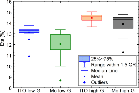
The study reveals that cells grown on ITO can match or exceed the performance of reference cells on conventional Mo back contacts, with a bifaciality of up to 60% measured for the ITO-based devices. Using scanning transmission electron microscopy, the team identified a thin (~3 nm) GaOx layer at the ACIGS/ITO interface, believed to provide a passivating effect at the back contact. Steepening the Ga-grading toward the rear interface further improved performance under both front- and rear-side illumination, pointing to an added rear-contact passivation effect achievable across absorber thicknesses ranging from 250 nm to 1 μm.
🔗 Read the full publication: https://doi.org/10.1109/JPHOTOV.2026.3668826
Read the full publication: https://doi.org/10.1109/JPHOTOV.2026.3668826
Why Ga-Grading Matters
Bifacial ACIGS solar cells on transparent back contacts offer a route to higher energy yield by capturing stray light reflected from the ground, but replacing the opaque Mo back contact has historically introduced performance penalties tied to increased rear-interface recombination. By identifying how Ga-grading can passivate the ITO/ACIGS interface, the study shows that:
Cells grown on ITO can equal or surpass the performance of reference cells on standard Mo back contacts, reaching up to 60% bifaciality
A thin, naturally forming GaOx layer at the ACIGS/ITO interface plays a passivating role at the back contact, as confirmed by STEM analysis
A steeper Ga-grading at the rear interface improves front- and rear-side performance alike, indicating an additional passivation benefit from the grading itself
This effect holds across a wide range of absorber thicknesses, from 250 nm to 1 μm
Compared with a flat Ga profile, the graded absorber achieves twice the current density under rear illumination and 12% higher current density under front illumination
Relevance for Ongoing CIGS Research
This work adds a practical, materials-level lever for closing the performance gap between bifacial and conventional ACIGS solar cells. By linking absorber grading design to back-contact passivation on transparent electrodes, the study gives researchers and manufacturers a concrete strategy for improving rear-side current collection as transparent back-contact architectures move toward wider adoption.
Open Access
In line with open science practices, the publication is openly available, enabling reproducibility and further exploration by the research community.
🔗 Access the article: https://zenodo.org/records/17610270